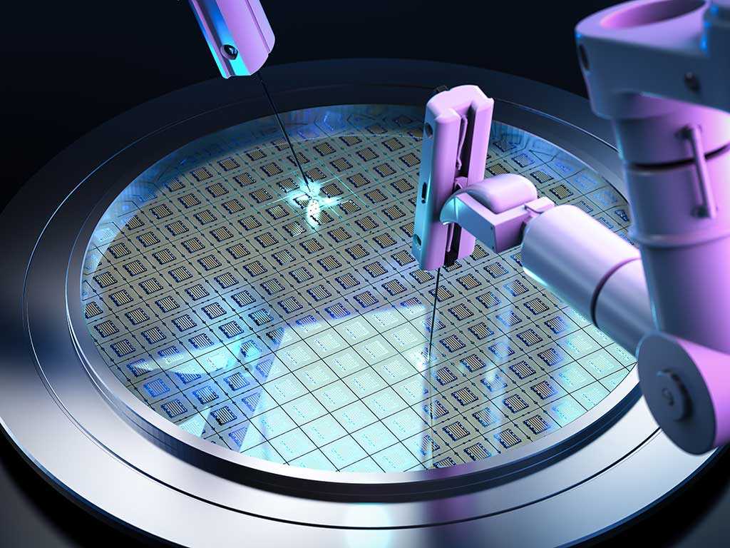
Ultra-high purity gases are essential throughout the semiconductor supply chain. In fact, for a typical fab, high purity gases represent the biggest material expenditure after silicon itself. In the wake of a global chip shortage, the industry is expanding faster than ever before – and its demand for high purity gases is increasing too. 1,2
The most commonly used bulk gases in semiconductor manufacturing are nitrogen, helium, hydrogen and argon.
Nitrogen
Constituting 78 percent of our atmosphere, nitrogen is incredibly abundant.3 It also happens to be chemically inert and electrically non-conductive. As a result, nitrogen has found its way into multiple industry sectors as a cost-effective inerting gas.
The semiconductor industry is a major consumer of nitrogen. A modern semiconductor fabrication plant can expect to use as much as 50,000 cubic meters of nitrogen per hour.4 In semiconductor manufacturing, nitrogen plays the role of a general-purpose inerting and purging gas, protecting sensitive silicon wafers from reactive oxygen and moisture in the air.
Helium
Helium is a noble gas. This means, like nitrogen, helium is chemically inert – but it also has the added advantage of being highly thermally conductive. This is particularly useful in semiconductor manufacturing, enabling it to efficiently conduct heat away from energetic processes and helping to protect them from thermal damage as well as unwanted chemical reactions.5,6
Hydrogen
Hydrogen is used extensively throughout electronics manufacturing, and semiconductor production is no exception. In particular, hydrogen is used for:
- Annealing: Silicon wafers are routinely heated to high temperatures and slowly cooled in order to repair (anneal) the crystal structure. Hydrogen is used to transfer heat uniformly to the wafer and assist the reconstruction of the crystal structure.
- Epitaxy: Ultra-high purity hydrogen is used as a reducing agent in the epitaxial deposition of semiconductor materials such as silicon and germanium.
- Deposition: Hydrogen can be incorporated into thin silicon films to make their atomic structure more disordered and help increase their electrical resistivity.
- Plasma Cleaning: Hydrogen plasma is particularly effective at removing tin contamination from light sources used in UV photolithography.7
Argon
Argon is another noble gas, so it exhibits low reactivity like nitrogen and helium. However, argon’s low ionisation energy earns its use in semiconductor applications. Because argon is comparatively easy to ionise, it’s commonly used as a primary plasma gas for etching and deposition reactions in semiconductor fabrication. In addition to this, argon is used in excimer lasers for UV lithography.8
Why Purity Matters
Conventionally, advances in semiconductor technology are achieved by dimensional scaling, with new generations of semiconductor technology characterised by smaller feature sizes. This produces multiple benefits: more transistors packed into a given volume, improved current flow, lower power consumption and faster switching.9,10
However, as the critical dimensions are driven downward, semiconductor devices become more and more delicate. In a world where the positions of single atoms are important, fault tolerance thresholds are incredibly tight. Modern semiconductor processes therefore demand the highest possible purity from process gases.
Air Products developed the BIP® range of gases to provide the highest possible level of gas purity for semiconductor applications. Crucially, BIP® gases offer not just high purity, but absolute minimum levels of critical impurities such as oxygen, moisture and hydrocarbons. Our proprietary BIP® technology – built into every cylinder – provides additional filtration of gas at point of use.
All BIP® gases have a minimum purity grade of 6.0 (99.9999% purity). We guarantee the market’s lowest levels of critical impurities: oxygen (≤10 ppb), moisture (≤ 20ppb) and total hydrocarbons (< 100 ppb). We supply specialty gases to the semiconductor industry in a range of supply modes to suit any consumption rate and applications.
Find out why Air Products is a world-leading supplier of ultra-pure gases to the semiconductor industry – contact a member of the Air Products team today.
References and Further Reading
- Ravi, S. Global Semiconductor Sales Increase 13.2% year-to-year in January. Semiconductor Industry Association [https://www.semiconductors.org/global-semiconductor-sales-increase-13-2-year-to-year-in-january/] (2021).
- Welle (www.dw.com), D. The EU’s microchip dilemma: Too little or too late? | DW | 29.04.2021. DW.COM [https://www.dw.com/en/the-eus-microchip-dilemma-too-little-or-too-late/a-57367537].
- Laboratory, S. U. H. I. on E. C. A. A. F.-P. S. B. A. B., NASA’s Jet Propulsion. The Atmosphere: Getting a Handle on Carbon Dioxide. Climate Change: Vital Signs of the Planet [https://climate.nasa.gov/news/2915/the-atmosphere-getting-a-handle-on-carbon-dioxide].
- Nitrogen Demand Increases for Semiconductor: How Safe Are You? PureAire Monitoring Systems Oxygen Monitor [https://www.pureairemonitoring.com/nitrogen-demand-increases-for-semiconductor-how-safe-are-you/] (2016).
- Helium Is Instrumental in Semiconductor Manufacturing. IER [https://www.instituteforenergyresearch.org/fossil-fuels/helium-is-instrumental-in-semiconductor-manufacturing/] (2021).
- Semiconductor Industry Association | Testimony of Carolyn Duran, Direction of Chemical Risk and Compliance, Global Sourcing and Procurement, Intel Corporation. [https://www.energy.senate.gov/services/files/BE7C9D0C-2043-4BBD-8313-C49CB6356C0E].
- Elg, D. T. Removal of Tin from Extreme Ultraviolet Collector Optics by an In-Situ Hydrogen Plasma. Ph.D. Thesis (2016).
- Tallents, G., Wagenaars, E. & Pert, G. Lithography at EUV wavelengths. Nature Photon 4, 809–811 (2010).
- Moore, G. E. No exponential is forever: but ‘Forever’ can be delayed! [semiconductor industry]. in 2003 IEEE International Solid-State Circuits Conference, 2003. Digest of Technical Papers. ISSCC. vol. 1 20–23 (IEEE, 2003).
- Orji, N. G. et al. Metrology for the next generation of semiconductor devices. Nat Electron 1, 532–547 (2018).
